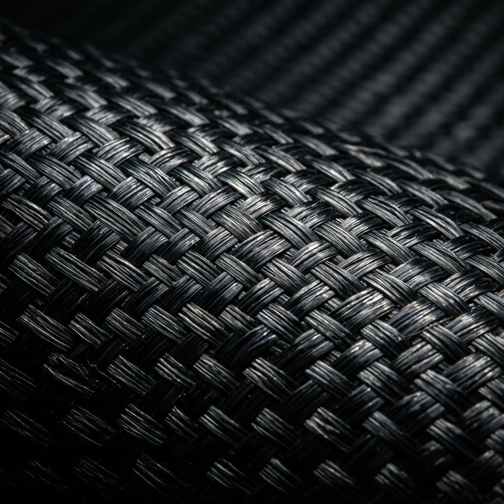
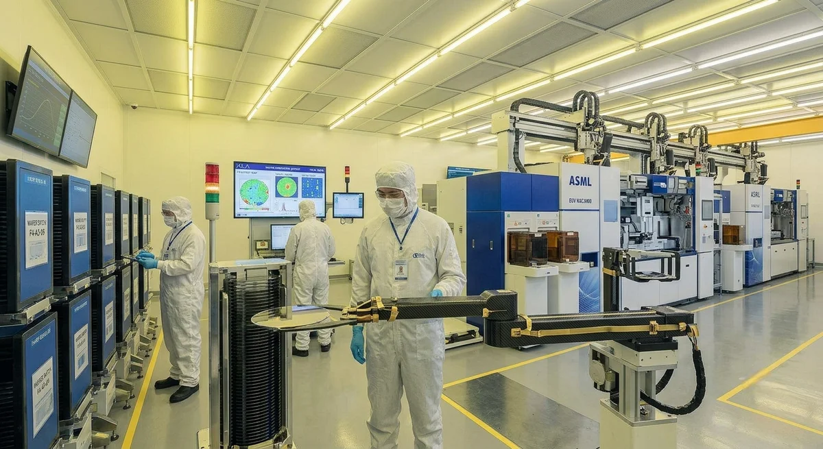
Carbon fiber composites are enabling higher precision and throughput in semiconductor manufacturing equipment through their unique combination of stiffness, light weight, thermal stability, and vibration damping. This article examines wafer handling end-effectors, reticle transport forks, ESD-safe components, and clean room compatibility for B2B buyers in the semiconductor equipment supply chain.
The semiconductor industry demands ever-increasing precision as manufacturing nodes shrink below 3 nm and wafer diameters remain at 300 mm with planned transition to 450 mm. In this ultra-precision environment, carbon fiber reinforced polymer (CFRP) composites have become an essential material for critical components in wafer handling equipment, reticle management systems, and clean room automation. The global market for carbon fiber components in semiconductor equipment is projected to reach $680 million by 2030, growing at a CAGR of 14.2%, driven by expansion of advanced fabrication facilities worldwide.
Carbon fiber offers a compelling property combination for semiconductor equipment: a specific stiffness (E/ρ) of approximately 8.5×10⁶ m²/s² — roughly 3.5 times that of aluminum and 5 times that of stainless steel. This translates directly to faster acceleration, reduced settling time, and higher throughput in robotic handling systems. Additionally, carbon fiber's near-zero coefficient of thermal expansion (CTE of −0.5 to +0.5 ppm/°C in the fiber direction) closely matches that of silicon (2.6 ppm/°C), minimizing thermal mismatch stress during wafer processing.
Wafer Handling End-Effectors
Wafer handling end-effectors (also called wafer forks or grippers) are the most critical carbon fiber components in semiconductor equipment. These must simultaneously satisfy extreme requirements for cleanliness, particle generation, stiffness, weight, and dimensional stability. Carbon fiber end-effectors now dominate the market for 300 mm wafer handling in etch, deposition, metrology, and lithography equipment.
| Parameter | CFRP End-Effector | Aluminum End-Effector | Ceramic (Al₂O₃) End-Effector |
|---|---|---|---|
| Tensile modulus (GPa) | 120-230 (unidirectional) | 69-73 | 300-400 |
| Density (g/cm³) | 1.55-1.60 | 2.70 | 3.90-3.95 |
| Specific stiffness (×10⁶ m²/s²) | 7.5-14.4 | 2.6-2.7 | 7.7-10.3 |
| CTE (ppm/°C) | −0.5 to 0.5 (fiber direction) | 23-24 | 5.4-8.5 |
| Thermal conductivity (W/m·K) | 50-200 (fiber direction) | 150-200 | 20-35 |
| Cycle time improvement | Baseline (fastest) | +25-40% slower | +15-30% slower |
| Natural frequency (Hz) | 80-150 (typical 300 mm fork) | 45-75 | 60-100 |
| Settling time to ±0.1 mm (ms) | 50-100 | 150-250 | 100-180 |
| Particle generation (per cycle) | < 0.01 particles @ 0.1 μm | 0.02-0.08 | 0.01-0.03 |
| Typical cost per unit | $1,500-3,500 | $400-800 | $2,500-6,000 |
| Service life (cycles) | 500,000-2,000,000 | 200,000-500,000 | 300,000-800,000 |
Key design considerations for CFRP wafer end-effectors include:
- Fiber architecture: Quasi-isotropic layups ([0/±45/90]s) are standard for general-purpose forks. High-stiffness forks use a [0₂/±45/0₂] layup with high-modulus (HM) carbon fiber (E = 390 GPa). The unidirectional plies in the 0° direction carry the bending load, while ±45° plies provide torsional stiffness and prevent edge delamination.
- Particle control: Bare CFRP surfaces can generate particles through fiber exposure and matrix micro-cracking. Standard mitigation strategies include parylene-C coating (0.5-5 μm), nickel-PTFE electroless plating (5-15 μm), or acrylic-based conformal coating. Coated end-effectors achieve Class 1 clean room compatibility (ISO Class 3) with particle generation rates below 0.01 particles per cycle at 0.1 μm.
- Electrostatic discharge (ESD): Bare carbon fiber has surface resistivity of 10³-10⁵ Ω/sq — inherently dissipative. However, coatings can increase surface resistivity to 10⁹-10¹² Ω/sq (insulative range), causing electrostatic buildup. ESD-safe coatings — carbon-nanotube-loaded acrylic or conductive PEEK — maintain surface resistivity in the dissipative range (10⁵-10⁹ Ω/sq) as required by SEMI E176 guidelines.
- Wafer edge contact: The edge-grip region uses compliant materials (PEEK, PTFE, or PAI pads) bonded to the carbon fiber fork tips. Contact force: 0.5-2.0 N per contact point. The CFRP substrate provides the global stiffness; the polymer pads distribute contact pressure and prevent wafer edge chipping.
Reticle Handling Components
Reticles (photomask plates) for advanced lithography are among the most expensive consumables in semiconductor manufacturing — a single EUV reticle costs $50,000-200,000. Their handling requires extreme precision and contamination control. Carbon fiber reticle transport forks and grippers have become the industry standard for EUV and DUV lithography systems.
- Reticle fork design: Dual-prong carbon fiber forks (typically 350-400 mm long, 12-18 mm wide per prong) with integrated vacuum channels. The fork must maintain flatness within ±50 μm across its entire length under a 1 kg payload. High-modulus pitch-based carbon fiber (E = 640-830 GPa, CTE = −1.5 ppm/°C) is used for the primary structural layer to achieve near-zero thermal deflection.
- Damping requirements: EUV reticle stages operate at accelerations up to 5 g with positioning tolerances of ±0.1 nm in X/Y. The carbon fiber fork's structural damping ratio (ζ = 0.01-0.03 for CFRP vs. 0.001-0.005 for aluminum) provides intrinsic vibration attenuation without additional dampers. Settling time for a CFRP fork is 40-80 ms, compared to 120-200 ms for aluminum equivalents.
- Outgassing control: EUV reticle handling requires ultra-low outgassing materials (AMC < 1 ppb). Carbon fiber reticle forks use high-purity epoxy resin systems (bisphenol A/F blends with < 0.1% residual solvent) and are vacuum-baked at 120-150°C for 8-24 hours prior to installation. Total mass loss (TML) per ASTM E595 is typically < 0.5%, with collected volatile condensable materials (CVCM) < 0.05%.
- Clean room particle qualification: Reticle transport forks undergo 200+ hour particle generation testing per SEMI S2 guidelines. Acceptable performance: < 0.005 particles per operation at 0.1 μm. Periodic cleaning with deionized water and megasonic agitation (1-3 MHz) restores particle performance.
| Parameter | Pitch-based HM CFRP Fork | PAN-based IM CFRP Fork | Aluminum Fork |
|---|---|---|---|
| Fiber modulus (GPa) | 640-830 | 290-395 | — |
| Fork stiffness (N/mm, cantilever) | 18-30 | 10-18 | 4-8 |
| Thermal deflection at ΔT = 1°C | < 0.5 μm | 1-3 μm | 15-25 μm |
| Natural frequency (first mode, Hz) | 110-160 | 80-120 | 45-70 |
| Damping ratio (ζ) | 0.02-0.035 | 0.01-0.025 | 0.001-0.005 |
| Mass per fork (g) | 65-90 | 80-120 | 180-250 |
| Cost per fork ($) | 3,000-6,000 | 1,800-3,500 | 500-1,200 |
ESD-Safe Structural Components in Semiconductor Equipment
Beyond wafer and reticle handling, carbon fiber is increasingly used for structural components within semiconductor equipment where ESD safety, stiffness, and weight are critical:
- Equipment frames and gantries: CFRP gantry beams in wafer inspection and metrology tools (e.g., KLA, Applied Materials e-beam systems). A 2-meter CFRP gantry beam (150×100 mm box section, 8 mm wall) weighs 8.5 kg vs. 42 kg for steel and 15.5 kg for aluminum, with 3× higher natural frequency. Dynamic compliance at the workpoint: 0.8 μm/N for CFRP vs. 2.5 μm/N for aluminum.
- Linear motion stages: CFRP moving platens and carriages in high-speed pick-and-place systems. Weight reduction of 60-70% vs. aluminum enables acceleration of 5-10 g with positioning accuracy of ±2 μm. Linear guide mounting surfaces are machined after cure or fitted with precision-ground aluminum/steel inserts bonded and pinned.
- Ion implanter components: Beamline components (scanning assemblies, electrostatic lens housings, and beam stops) benefit from carbon fiber's combination of dimensional stability, low outgassing, and radiation resistance. Carbon fiber beam stops are replacing graphite in high-current implanters, offering 3-5× longer service life with reduced particle generation.
- Chemical mechanical planarization (CMP) heads: CFRP CMP carrier heads (membrane backing plates) provide the required flatness (< 5 μm across 300 mm) while weighing 60% less than aluminum heads. Reduced inertial forces enable faster platen acceleration and improved within-wafer non-uniformity (WIWNU) of < 2% at 3σ.
Clean Room Compatibility and Certification
Carbon fiber components for semiconductor equipment must meet strict clean room compatibility standards:
| Requirement | Standard/Method | Acceptable Limit | Typical CFRP Performance |
|---|---|---|---|
| Particle generation | SEMI S2 / IEST-RP-CC003 | < 0.01 particles/cycle @ ≥0.1 μm | 0.003-0.008 |
| Surface resistivity | SEMI E176 / ANSI/ESD STM11.11 | 10⁵-10⁹ Ω/sq | 10⁴-10⁶ (uncoated); 10⁵-10⁸ (ESD coating) |
| Outgassing (TML) | ASTM E595 | < 1.0% TML, < 0.1% CVCM | 0.3-0.6% TML, 0.01-0.05% CVCM |
| VOC emission | ISO 16000-6 | < 10 μg/m³ (individual VOCs) | < 5 μg/m³ (after vacuum bake) |
| Chemical resistance | SEMI F104 / immersion | No degradation in process chemicals | Resistant to DI water, IPA, dilute HF (10:1); epoxy attacked by NMP, TMAH at > 50°C |
| Thermal stability | SEMI E154 | Dimensional drift < 1 μm/°C | 0.1-0.5 μm/°C (fiber-dominated orientation) |
FAQ
Why is carbon fiber preferred over aluminum for wafer handling end-effectors in advanced semiconductor fabs?
Carbon fiber offers three decisive advantages for wafer handling at leading-edge nodes (7 nm and below). First, specific stiffness: CFRP's E/ρ ratio of 7.5-14.4×10⁶ m²/s² enables 25-40% faster robot cycle times compared to aluminum (2.6-2.7×10⁶). Second, thermal stability: CFRP's CTE of −0.5 to 0.5 ppm/°C in the fiber direction is 50-100× lower than aluminum's 23-24 ppm/°C, meaning temperature fluctuations of ±0.5°C in the clean room cause < 0.5 μm deflection in a CFRP fork vs. 12-15 μm in aluminum — a critical difference for sub-10 nm overlay alignment. Third, vibration damping: CFRP's structural damping ratio (0.01-0.03) is 5-30× higher than aluminum (0.001-0.005), reducing settling time after high-acceleration moves from 150-250 ms (aluminum) to 50-100 ms (CFRP). While the upfront cost is 3-5× higher, total cost of ownership is typically lower due to 2-4× longer service life and higher throughput.What coating or surface treatment is used on carbon fiber semiconductor components to prevent particle shedding?
Multiple coating strategies are used depending on the application. For wafer end-effectors, parylene-C conformal coating (0.5-5 μm thickness) is the most common — it provides a pinhole-free, low-friction surface with excellent adhesion to CFRP. Parylene-C has a surface resistivity of 10¹³-10¹⁵ Ω/sq (insulative), so ESD-safe variants use parylene with carbon nanotube loading or an underlying conductive layer. For reticle forks, nickel-PTFE electroless plating (5-15 μm) provides wear resistance and particle suppression, with surface resistivity tunable to 10⁵-10⁹ Ω/sq by controlling the PTFE particle content (15-30% by volume). For structural frames and gantries that do not contact wafers directly, a high-build epoxy primer (25-50 μm) with ESD-safe polyurethane topcoat (50-80 μm) is typical. All coatings must pass 100-cycle IPA wipe testing and 24-hour DI water immersion without blistering or delamination. Uncoated CFRP is generally acceptable only in non-product-contact areas of atmospheric robots in older-generation fabs.How does carbon fiber's thermal expansion behavior affect reticle positioning accuracy in EUV lithography?
In EUV lithography systems, reticle positioning accuracy must be maintained to within ±0.1 nm in X/Y during scanning. Temperature control in the EUV reticle chamber is ±0.01°C, but localized heating from the reticle stage motors and the scanning beam creates transient thermal gradients. A carbon fiber reticle fork made from pitch-based high-modulus fiber (E = 640-830 GPa, CTE = −1.5 ppm/°C) experiences thermal deflection of < 0.5 μm per 1°C temperature change across the fork length. For comparison, an aluminum fork would deflect 15-25 μm under the same gradient — 30-50× more. The negative CTE of pitch-based carbon fiber (−1.5 ppm/°C) can be designed to cancel the positive CTE of the resin matrix, creating zero-CTE laminates (< ±0.1 ppm/°C). This is achieved through balanced symmetric layups with specific fiber volume fractions. The near-zero CTE ensures that reticle-to-stage positioning errors from thermal drift remain < 0.05 nm during a typical 30-minute EUV exposure sequence.What specific grades of carbon fiber are used in semiconductor equipment components?
Three grades dominate semiconductor applications. (1) Intermediate modulus PAN-based fiber (E = 290-395 GPa, e.g., Toray T800S/T1100G, Hexcel IM7/IM10) — used for wafer end-effectors and general structural components. These offer the best balance of stiffness, strength, and cost. (2) High-modulus pitch-based fiber (E = 640-830 GPa, e.g., Mitsubishi K13D2U, Nippon Graphite YS-95A) — used exclusively for reticle forks and metrology frame components requiring ultra-high stiffness and near-zero CTE. Pitch-based fiber costs $500-2,000/kg — 5-20× more than PAN-based fiber ($30-120/kg for aerospace-grade). (3) High-strength PAN-based fiber (E = 230-250 GPa, e.g., Toray T700S) — used for non-critical structural brackets and covers where lower stiffness is acceptable. The carbon fiber precursor (PAN vs. pitch) selection depends on the stiffness requirement: pitch-based for E > 600 GPa, PAN-based for E < 400 GPa. Hybrid layups combining both fiber types in the same component (pitch fiber in 0° plies, PAN fiber in ±45° plies) are common in reticle fork designs.Part of topic
Related Articles
- Carbon Fiber Mooring for Floating Offshore Wind: Fatigue and Corrosion in Deep Water
- Carbon Fiber Bicycle Frame Optimization: Layup Design and Manufacturing for Competitive Racing
- Carbon Fiber CFRP Retrofit for Infrastructure: Bridge and Building Seismic Strengthening
- Carbon Fiber Medical Imaging Equipment: Lightweight Gantry and Couch Structures for MRI/CT
- Carbon Fiber EV Battery Enclosures: Crash Safety and Electromagnetic Shielding Design
- Carbon Fiber Structures for Low-Altitude Economy: UAV Airframes and eVTOL Components
Interested in Our Products?
Contact our team for competitive pricing and technical specifications.
Get a QuoteRelated Products
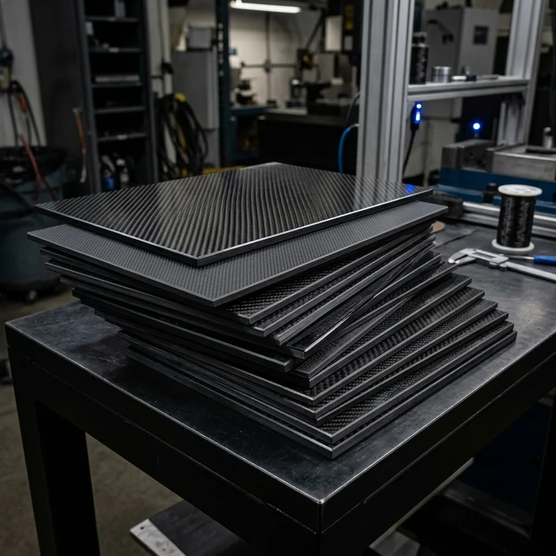
Carbon fiber standard plate-3k stripe
Lightweight, ultra-rigid standard sheets for drone fuselages, robot housings, facades and structural applications.
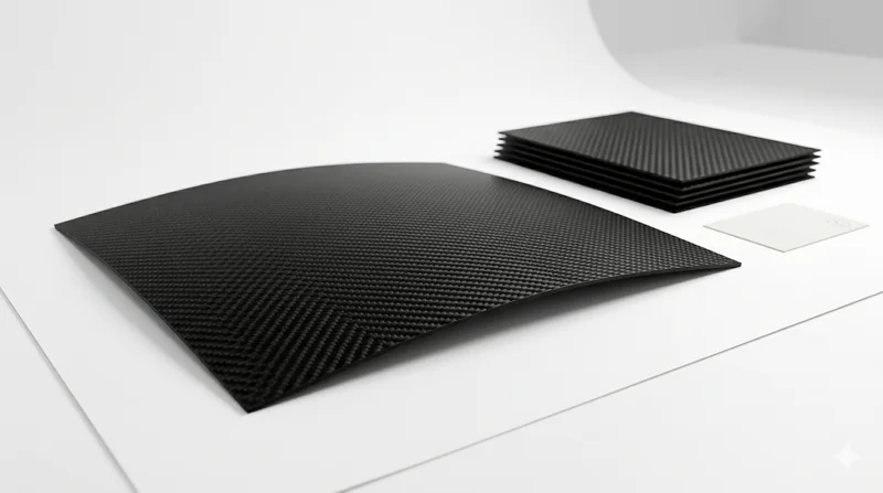
Carbon Fiber Plate — 3K Twill T700 1.5mm
Thin 1.5mm carbon fiber plate with 3K twill weave surface. Lightweight and stiff, commonly used for covers, panels, drone bodies, and applications requiring a premium aesthetic appearance.
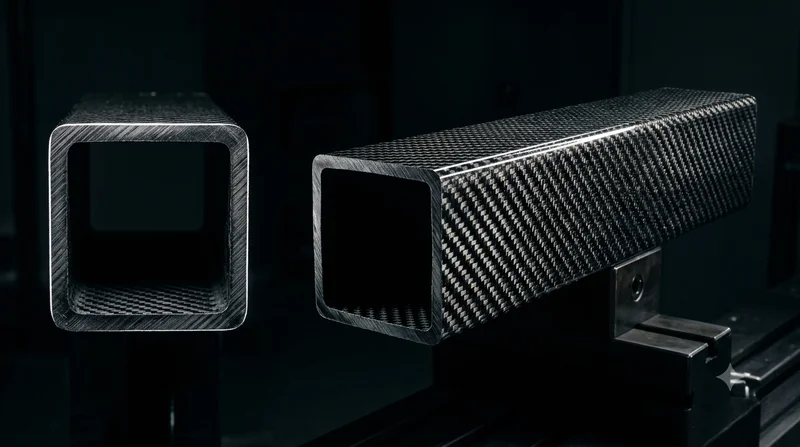
Square Carbon Fiber Tube — 3K Twill T700
Square cross-section carbon fiber tube manufactured with 3K twill weave for torsional strength. Preferred for structural frames, trusses, and support columns where rectangular geometry offers design flexibility.
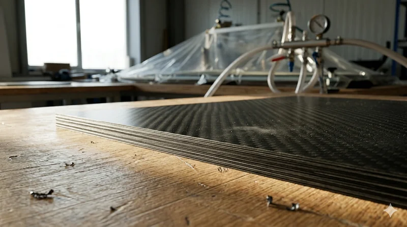
Carbon Fiber Plate — 3K Twill T700 3.0mm
Medium-thickness 3.0mm carbon fiber plate offering significantly higher load capacity while maintaining attractive 3K twill finish. Suitable for structural brackets, reinforcement plates, and load-bearing panels.
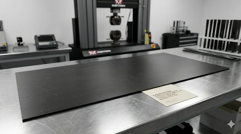
Carbon Fiber Plate — UD Unidirectional T700
Unidirectional carbon fiber plate with all fibers oriented in a single direction for maximum strength along the fiber axis. Essential for structural reinforcements, splints, and applications where load direction is predictable.